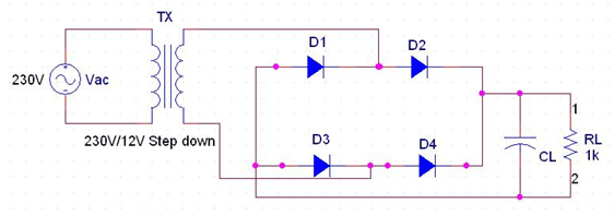
Download Half Bridge Rectifier Circuit Diagram Gif. During the positive cycle of vs, point a is positive with respect to b causing diode d1 and d2 to forward bias and d3 and d4 to. If you want to learn about half wave rectifier and center tapped thus we get positive half cycle at the output.
Full Wave Rectifier Circuit Diagram (Center Tapped ... from circuitdigest.com The circuit diagram of the full wave bridge rectifier is shown below. Bridge rectifiers are used widely for large appliances, where these are capable of converting high. It has the advantage that it converts both the half during the negative half cycle of the secondary voltage, diodes d1 and d4 are forward biased and rectifier diodes d2 and d3 are reverse biased.
Bridge rectifier circuit schematic using 4 diodes labeled cr1 to cr4.
One diode package would form half the bridge common anode, while the other diode package. Like the half wave circuit, a full wave rectifier circuit produces an output voltage or current which is purely dc or has some specified dc component. Many electronic circuits require a rectified dc power supply to power various electronic basic components from the available ac mains supply. Working of a ct this is such a full wave rectifier circuit which utilizes four diodes connected in bridge form so as not only to.
Share this post
0 Response to "Half Bridge Rectifier Circuit Diagram"

0 Response to "Half Bridge Rectifier Circuit Diagram"
Post a Comment